| CPC H01L 33/36 (2013.01) [H01L 33/38 (2013.01); H01L 33/387 (2013.01); H01L 33/46 (2013.01); H01L 33/60 (2013.01); H01L 33/62 (2013.01); H01L 2933/0016 (2013.01); H01L 2933/0025 (2013.01); H01L 2933/0058 (2013.01); H01L 2933/0066 (2013.01)] | 18 Claims |
|
1. An optoelectronic device comprising an optoelectronic semiconductor chip configured to emit electromagnetic radiation, wherein the optoelectronic semiconductor chip comprises:
a first semiconductor layer of a first conductivity type;
a second semiconductor layer of a second conductivity type;
first and second current spreading layers;
a dielectric mirror layer; and
a plurality of first electrical connecting elements and a plurality of second electrical connecting elements;
wherein:
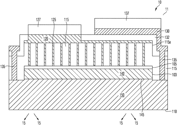
the first semiconductor layer and the second semiconductor layer are stacked one on top of the other, and the first semiconductor layer is patterned to form a mesa;
the electromagnetic radiation emitted by the optoelectronic semiconductor chip is output via a first main surface of the second semiconductor layer;
the first current spreading layer is arranged on a side of the first semiconductor layer facing away from the second semiconductor layer;
the dielectric mirror layer is arranged between the first semiconductor layer and the first current spreading layer, and is further arranged over a mesa flank, covering the same;
the plurality of first electrical connecting elements extends through the dielectric mirror layer and are configured to electrically connect the first semiconductor layer to the first current spreading layer;
the second current spreading layer is arranged on a side of the first semiconductor layer facing away from the second semiconductor layer and is electrically connected to the second semiconductor layer via the plurality of second electrical connecting elements, and the number of first electrical connecting elements is greater than the number of second electrical connecting elements, wherein the second current spreading layer is arranged at a greater distance from the first semiconductor layer than the first current spreading layer,
wherein the optoelectronic device further comprises first and second contact elements, wherein the first contact element is connected to the first current spreading layer, the second contact element is connected to the second current spreading layer, and the first and second contact elements are arranged on a side of the first semiconductor layer facing away from the second semiconductor layer,
wherein the optoelectronic semiconductor chip further comprises a first contact post and a second contact post, wherein the first contact post is connected to the first contact element and the second contact post is connected to the second contact element, wherein the second contact element is arranged between the second contact post and the second current spreading layer.
|