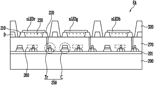
| CPC H01L 33/24 (2013.01) [H01L 27/156 (2013.01); H01L 33/007 (2013.01); H01L 33/0075 (2013.01); H01L 33/16 (2013.01); H01L 33/325 (2013.01); H01L 33/38 (2013.01); H01L 33/44 (2013.01); G09G 3/32 (2013.01); G09G 2300/0452 (2013.01); G09G 2310/0278 (2013.01); H01L 25/0753 (2013.01); H01L 27/1214 (2013.01); H01L 2224/95085 (2013.01); H01L 2933/0016 (2013.01); H01L 2933/0025 (2013.01)] | 21 Claims |

|
1. A light emitting device, comprising:
a substrate;
a data line on the substrate;
a first electrode and a second electrode spaced apart from each other on the substrate;
an LED disposed on and over the first and second electrodes, the LED having a first end on the first electrode, a second end on the second electrode, and an LED insulating film surrounding at least a part of an outer circumferential surface of the LED and exposing opposite side surfaces of the first and second ends;
a first insulating layer between the substrate and the LED;
a first contact electrode and a second contact electrode respectively disposed on the first and second ends of the LED; and
a wall-shaped pixel defining layer adjacent to the first and second electrodes, wherein
the first contact electrode is in contact with the side surface of the first end of the LED,
the second contact electrode is in contact with the side surface of the second end of the LED, and
at least a part of the wall-shaped pixel defining layer overlaps at least a part of the data line.
|