| CPC H01L 31/0304 (2013.01) [H01L 31/02327 (2013.01); H01L 31/0328 (2013.01); H01L 31/109 (2013.01); H01S 5/02461 (2013.01); H01S 5/3211 (2013.01); H01S 5/3213 (2013.01); H01S 5/021 (2013.01); H01S 5/026 (2013.01); H01S 5/1032 (2013.01); Y02E 10/544 (2013.01)] | 20 Claims |

|
1. A semiconductor device comprising:
a cladding layer defining a longitudinal direction transverse to a surface of the cladding layer and a lateral direction parallel to the cladding layer;
a silicon semiconductor layer adjacent to the cladding layer;
a buried oxide layer adjacent to the silicon semiconductor layer; and
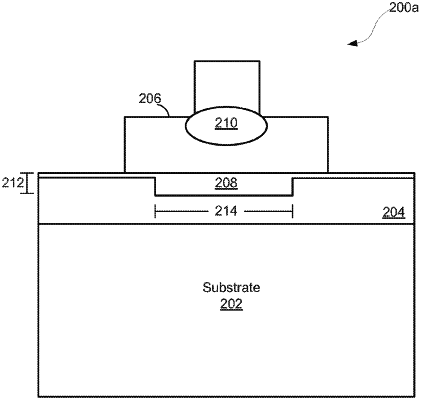
a III-V semiconductor layer on the surface of the cladding layer, the III-V semiconductor layer having a lateral width that is wider than a narrow lateral width of the cladding layer, the III-V semiconductor layer having an active region with light confined in the III-V semiconductor layer by the cladding layer, the light being confined in the longitudinal direction transverse to the surface of the cladding layer.
|