| CPC H01L 31/024 (2013.01) [H01L 27/14634 (2013.01)] | 10 Claims |
|
1. A semiconductor device, comprising:
a substrate that comprises metal wiring;
a solid-state imaging element mounted on a surface of the substrate; and
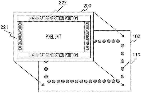
an adhesive portion having a specific thermal conductivity, wherein the adhesive portion adheres a specific region on one surface of the solid-state imaging element to the substrate, wherein
the substrate comprises an insulating film on the surface,
the insulating film comprises an exposed portion that opens in the specific region to expose the metal wiring, and
the adhesive portion adheres the specific region of the solid-state imaging element to the metal wiring of the substrate.
|