| CPC H01L 29/945 (2013.01) [H01L 21/76834 (2013.01); H01L 21/7687 (2013.01); H01L 21/76877 (2013.01); H01L 23/5223 (2013.01); H01L 23/5226 (2013.01); H01L 28/57 (2013.01); H01L 28/65 (2013.01); H01L 28/75 (2013.01); H10B 53/30 (2023.02)] | 18 Claims |
|
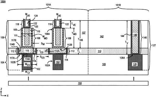
1. A device comprising:
a first region comprising:
a first conductive interconnect within a first dielectric in a first level; and
a second level above the first level, the second level comprising:
an electrode structure on the first conductive interconnect, the electrode structure comprising:
a first conductive hydrogen barrier layer; and
a first conductive fill material on the first conductive hydrogen barrier layer, wherein the electrode structure comprises a first lateral thickness;
an etch stop layer comprising an insulator, the etch stop layer laterally surrounding the electrode structure;
a second dielectric on the etch stop layer, the second dielectric comprising an amorphous, greater than 90% film density hydrogen barrier material;
a trench within the second dielectric, the trench on the electrode structure;
a non-planar capacitor within the trench, the non-planar capacitor comprising:
a first electrode along a base and a sidewall of the trench, wherein the first electrode is on the electrode structure;
a dielectric layer comprising a ferroelectric material or a paraelectric material substantially conformal to and extending over the first electrode on to an uppermost surface of the second dielectric; and
a second electrode in contact with the dielectric layer; and
a via electrode on the second electrode, the via electrode comprising:
a second conductive hydrogen barrier layer comprising a lateral portion in contact with the second electrode and substantially vertical portions connected to the lateral portion; and
a second conductive fill material adjacent to the second conductive hydrogen barrier layer; and
a second region adjacent to the first region, the second region comprising:
a second conductive interconnect within the first level;
a third dielectric on the etch stop layer, the third dielectric directly adjacent to the second dielectric, wherein the third dielectric comprises a less than 90% film density material; and
a via structure on the second conductive interconnect, the via structure laterally in contact with the third dielectric.
|