| CPC H01L 29/93 (2013.01) [H01L 29/0649 (2013.01); H01L 29/2003 (2013.01); H01L 29/778 (2013.01)] | 20 Claims |

|
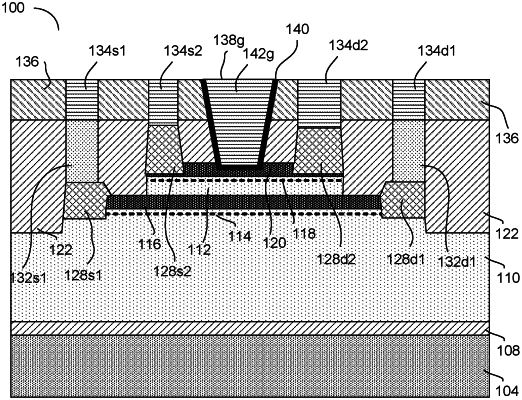
1. A variable capacitance device comprising:
a first two-dimensional electron gas (2DEG) region within a first material layer comprising Ga and N;
a first polarization material layer over the first material layer;
a first source and a first drain coupled to the first material layer, wherein the first source and the first drain comprise a Group III element, N, and a donor impurity;
a second 2DEG region within a second material layer comprising Ga and N, wherein the second material layer is over the first material layer and wherein a thickness of the first material layer is greater than a thickness of the second material layer;
a second polarization material layer over the second material layer, wherein a thickness of the first polarization material layer is greater than a thickness of the second polarization material layer;
a second source and a second drain coupled to the second material layer, wherein the second source and the second drain comprise a Group III element, N, and a donor impurity;
and a gate electrode over the second material layer.
|