US 12,034,083 B2
Nonvolatile storage element and analog circuit provided with same
Toshiro Sakamoto, Tokyo (JP); Satoshi Takehara, Tokyo (JP); Yoshiro Yamaha, Tokyo (JP); and Makoto Kobayashi, Tokyo (JP)
Assigned to ASAHI KASEI MICRODEVICES CORPORATION, Tokyo (JP)
Filed by ASAHI KASEI MICRODEVICES CORPORATION, Tokyo (JP)
Filed on Feb. 10, 2023, as Appl. No. 18/108,519.
Application 18/108,519 is a continuation of application No. 16/649,175, granted, now 11,611,000, previously published as PCT/JP2017/036017, filed on Oct. 3, 2017.
Prior Publication US 2023/0197861 A1, Jun. 22, 2023
Int. Cl. H01L 21/00 (2006.01); H01L 21/28 (2006.01); H01L 29/423 (2006.01); H01L 29/66 (2006.01); H01L 29/788 (2006.01); H10B 41/30 (2023.01)
CPC H01L 29/7883 (2013.01) [H01L 29/40114 (2019.08); H01L 29/42324 (2013.01); H01L 29/66825 (2013.01); H10B 41/30 (2023.02)] 20 Claims
OG exemplary drawing
 
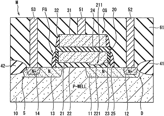
1. A nonvolatile storage element comprising:
a substrate;
a gate region having a charge holding region and an insulator surrounding an entire surface of the charge holding region;
a drain region formed in one of both sides of a lower portion of the gate region; and
a source region formed in another one of both the sides,
wherein a halogen is distributed in the insulator to cover an entire surface of an upper surface of the charge holding region.