| CPC H01L 29/7869 (2013.01) [H01L 21/02422 (2013.01); H01L 21/02488 (2013.01); H01L 21/02554 (2013.01); H01L 21/02565 (2013.01); H01L 21/0262 (2013.01); H01L 21/02631 (2013.01); H01L 27/1225 (2013.01); H01L 27/127 (2013.01); H01L 29/045 (2013.01); H01L 29/24 (2013.01); H01L 29/66969 (2013.01); H01L 29/78648 (2013.01); H01L 29/78696 (2013.01)] | 4 Claims |

|
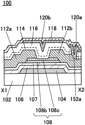
1. A method for manufacturing a semiconductor device, comprising the steps of:
forming a first insulating film;
forming a first oxide semiconductor film by a sputtering method over the first insulating film;
forming a second insulating film over the first oxide semiconductor film; and
forming a first gate electrode comprising a second oxide semiconductor film by a sputtering method over the second insulating film,
wherein, in the step of forming the first and the second oxide semiconductor film, an oxygen gas mixed with an inert gas is introduced into a deposition chamber,
wherein, in the step of forming the second oxide semiconductor film, a volume flow rate percentage of the oxygen gas to the oxygen gas and the inert gas is higher than or equal to 50% and lower than 100%, and
wherein, a volume flow rate percentage of the oxygen gas in the step of forming the first oxide semiconductor film is lower than the volume flow rate percentage of the oxygen gas in the step of forming the second oxide semiconductor film.
|