| CPC H01L 29/7851 (2013.01) [H01L 21/76871 (2013.01); H01L 21/823431 (2013.01); H01L 21/823475 (2013.01); H01L 23/481 (2013.01); H01L 23/528 (2013.01); H01L 23/5286 (2013.01); H01L 23/535 (2013.01); H01L 27/0886 (2013.01); H01L 29/66795 (2013.01); H01L 29/41791 (2013.01)] | 20 Claims |

|
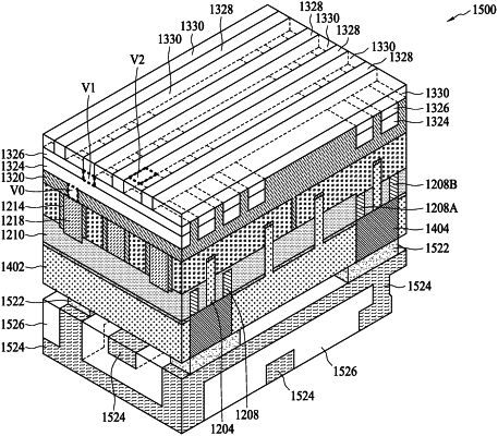
1. A semiconductor device, comprising:
a substrate;
a dielectric region situated on the substrate;
a first fin structure protruding from the substrate and the dielectric region;
a second fin structure protruding from the substrate and the dielectric region, the second fin structure extending parallel to the first fin structure;
a plurality of conductive regions situated on the dielectric region;
a first conductive rail situated within the dielectric region, the first conductive rail being electrically connected to a first conductive region of the plurality of conductive regions, wherein a first side of the first conductive rail faces the first fin structure, and a second side of the first conductive rail opposite to the first side faces the second fin structure; the first conductive region is formed on the first fin structure, and extends beyond the second side of the first conductive rail; and
a conductive structure penetrating through the substrate and formed under the first conductive rail, the conductive structure being electrically connected to the first conductive rail.
|