| CPC H01L 29/7813 (2013.01) [H01L 21/0465 (2013.01); H01L 29/0623 (2013.01); H01L 29/063 (2013.01); H01L 29/1095 (2013.01); H01L 29/1608 (2013.01); H01L 29/36 (2013.01); H01L 29/4236 (2013.01); H01L 29/66068 (2013.01); H01L 29/66727 (2013.01); H01L 29/66734 (2013.01); H01L 29/7827 (2013.01); H01L 29/41766 (2013.01)] | 15 Claims |
|
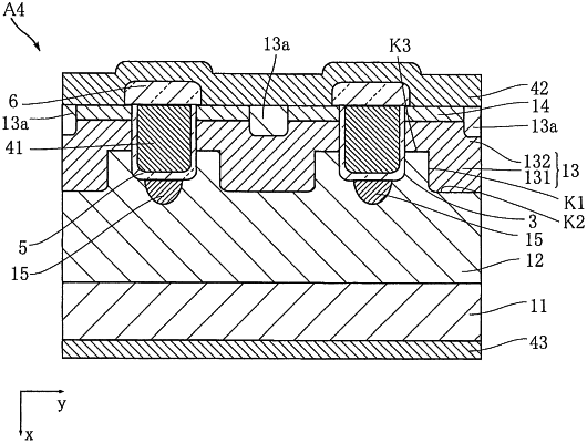
1. A semiconductor device comprising:
a layer of semiconductor having a first face and a second face opposite to the first face, the first face being provided with a first trench and a second trench adjacent to the first trench;
a first gate electrode provided in the first trench;
a second gate electrode provided in the second trench;
a first insulating layer provided in the first trench for insulating the layer of semiconductor and the first gate electrode from each other; and
a second insulating layer provided in the second trench for insulating the layer of semiconductor and the second gate electrode from each other;
wherein the layer of semiconductor includes a first semiconductor layer of a first conductivity type, and a second semiconductor layer of a second conductivity type opposite to the first conductivity type, the second semiconductor layer being generally closer to the first face than is the first semiconductor layer,
wherein each of the first trench and the second trench extends through the second semiconductor layer and reaches the first semiconductor layer,
the second semiconductor layer includes: a close portion that is close to the second face of the layer of semiconductor and disposed between the first trench and the second trench; and a sublayer disposed farther from the second face of the layer of semiconductor than is the close portion,
the second semiconductor layer includes a first channel region formed along the first trench and in contact with the first semiconductor layer and a second channel region formed along the second trench and in contact with the first semiconductor layer,
the close portion is spaced apart from each of the first trench and the second trench so that an upper interface of the close portion is at a same or substantially same height with a lower interface of each of the first channel region and the second channel region, and
the layer of semiconductor further comprises a first semiconductor region and a second semiconductor region of the second conductivity type, the first semiconductor region being formed around a bottom portion of the first trench, the second semiconductor region being formed along a bottom portion of the second trench,
the first trench and the second trench are symmetrical with respect to a center line of the close portion.
|