| CPC H01L 29/7397 (2013.01) [H01L 29/0619 (2013.01); H01L 29/0696 (2013.01); H01L 29/0804 (2013.01); H01L 29/0821 (2013.01); H01L 29/1004 (2013.01); H01L 29/16 (2013.01); H01L 29/41708 (2013.01); H01L 29/42304 (2013.01); H01L 29/4236 (2013.01); H01L 29/456 (2013.01); H01L 29/4916 (2013.01); H01L 29/4958 (2013.01); H01L 29/4966 (2013.01); H01L 29/6634 (2013.01); H01L 29/66348 (2013.01); H01L 29/402 (2013.01); H01L 29/42376 (2013.01); H01L 29/7396 (2013.01)] | 20 Claims |
|
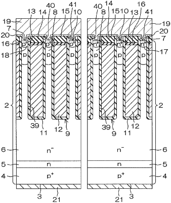
1. A semiconductor device comprising:
a first conductive-type semiconductor layer;
a second conductive-type base region that is arranged in a front surface portion of the first conductive-type semiconductor layer;
a plurality of trenches that extend from a front surface of the first conductive-type semiconductor layer beyond a bottom portion of the second conductive-type base region, an active region being defined between the plurality of trenches and having an upper surface at the front surface portion of the first conductive-type semiconductor layer;
a plurality of first conductive-type emitter regions, that are arranged in the active region, each connecting the trenches that are adjacent to each other such that each of the first conductive type emitter regions is not divided while extending from one of the trenches to another of the trenches and each having an upper surface at the front surface portion of the first conductive-type semiconductor layer;
a gate electrode that is embedded in the trenches;
an embedding insulating film that is embedded in the trenches on the gate electrode and that has an upper surface in the same height position as the front surface of the first conductive type semiconductor layer or in a height position lower than the front surface portion of the first conductive-type semiconductor layer;
a second conductive-type base contact region that is selectively arranged in the active region and that is connected to the second conductive-type base region at a bottom portion of the second conductive-type base contact region;
wherein the upper surface of the active region and the upper surface of the embedding insulating film providing a substantially flat surface;
an emitter electrode that is disposed over the substantially flat surface and that is electrically connected to the second conductive-type base region and the first conductive type emitter regions,
the trenches are formed in a stripe shape,
the first conductive-type emitter regions are formed in a stripe shape perpendicularly intersecting the trenches in the stripe shape,
the plurality of first conductive-type emitter regions and a plurality of the second conductive- type base contact regions are alternately arranged along the trenches in the active region such that the plurality of first conductive-type emitter regions and the plurality of the second conductive-type base contact regions are divided by one another,
the emitter electrode includes a first surface in contact with the plurality of first conductive- type emitter regions and the plurality of the second conductive-type base contact regions and a second surface opposite to the first surface,
the first surface of the emitter electrode extends continuously and flat across the plurality of striped trenches and a plurality of the active regions between the plurality of striped trenches, the first conductive-type emitter regions are formed deeper than the embedding insulating film and cross the boundary between the embedding insulating film and the gate electrode in a depth direction of the trench such that each of the first conductive-type emitter region is opposite to the embedding insulating film and the gate electrode in a lateral direction perpendicular to the depth direction,
the second conductive-type base contact region is formed shallower than the embedding insulating film such that a boundary between the second conductive-type base contact region and the second conductive-type base region continuously extending from one of the trenches to another of the trenches at a position closer to the front surface of the first conductive-type semiconductor layer than a boundary between the embedding insulating film and gate electrode, and
the second conductive-type base contact region is not opposite to the gate electrode in the lateral direction.
|