| CPC H01L 29/6681 (2013.01) [H01L 21/02054 (2013.01); H01L 29/6653 (2013.01); H01L 29/6656 (2013.01); H01L 29/7848 (2013.01)] | 20 Claims |
|
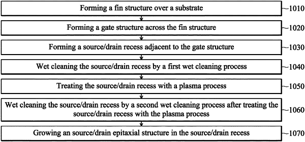
1. A method for forming a semiconductor structure, comprising:
forming a gate structure over a substrate;
forming a spacer on a sidewall of the gate structure;
forming a source/drain recess beside the spacer;
treating the source/drain recess and partially removing the spacer in a first cleaning process, wherein the first cleaning process removes metal residue;
treating the source/drain recess with a plasma process after performing the first cleaning process;
treating the source/drain recess in a second cleaning process after treating the source/drain recess with the plasma process, wherein the first cleaning process and the second cleaning process use different etchants; and
forming a source/drain structure in the source/drain recess after performing the second cleaning process.
|