| CPC H01L 29/6656 (2013.01) [H01L 21/30604 (2013.01); H01L 21/31144 (2013.01); H01L 21/76816 (2013.01); H01L 21/76831 (2013.01); H01L 21/76897 (2013.01); H01L 21/823418 (2013.01); H01L 21/823431 (2013.01); H01L 21/823468 (2013.01); H01L 21/823475 (2013.01); H01L 27/0886 (2013.01); H01L 29/0653 (2013.01); H01L 29/41791 (2013.01); H01L 29/4232 (2013.01); H01L 29/42392 (2013.01); H01L 29/66553 (2013.01); H01L 29/785 (2013.01); H01L 29/78696 (2013.01); H01L 2029/7858 (2013.01)] | 19 Claims |
|
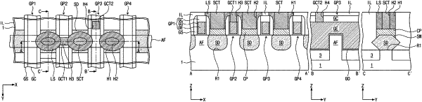
1. A semiconductor device, comprising:
a gate pattern crossing over a substrate, the gate pattern including a gate insulating layer, a gate electrode, and a gate capping pattern sequentially stacked on the substrate;
a gate spacer covering a sidewall of the gate pattern;
a source/drain pattern on the substrate, the source/drain pattern being adjacent to the sidewall of the gate pattern;
a contact pad on the source/drain pattern, a top surface of the contact pad being lower than a top surface of the gate electrode, wherein the contact pad directly contacts the gate spacer and is disposed on a top surface of the source/drain pattern;
a source/drain contact plug on the contact pad; and
a protection spacer enclosing the source/drain contact plug between the gate spacer and the source/drain contact plug,
wherein, when viewed in a plan view, the protection spacer has a ring shape having an inner diameter and an outer diameter,
wherein the inner diameter of the protection spacer remains substantially constant as a distance from the substrate increases, and
wherein the outer diameter of the protective spacer changes along a lateral surface of the gate spacer as the distance from the substrate increases.
|
|
10. A semiconductor device, comprising:
a gate pattern crossing over a substrate, the gate pattern including a gate insulating layer, a gate electrode, and a gate capping pattern sequentially stacked on the substrate;
a gate spacer covering a sidewall of the gate pattern;
a source/drain pattern on the substrate, the source/drain pattern being adjacent to the sidewall of the gate pattern;
a contact pad on the source/drain pattern, a top surface of the contact pad being lower than a top surface of the gate electrode, wherein the contact pad directly contacts the gate spacer and is disposed on a top surface of the source/drain pattern;
a source/drain contact plug on the contact pad; and
a protection spacer enclosing the source/drain contact plug between the gate spacer and the source/drain contact plug,
wherein, when viewed in a plan view, the protection spacer has a ring shape having an inner diameter and an outer diameter, and
wherein a difference between the inner diameter and the outer diameter of the protective spacer along a lateral surface of the gate spacer increases as a distance from the substrate increases.
|
|
15. A semiconductor device, comprising:
a gate pattern crossing over a substrate, the gate pattern including a gate insulating layer, a gate electrode, and a gate capping pattern sequentially stacked on the substrate;
a gate spacer covering a sidewall of the gate pattern;
a source/drain pattern on the substrate, the source/drain pattern being adjacent to the sidewall of the gate pattern;
a contact pad on the source/drain pattern, a top surface of the contact pad being lower than a top surface of the gate electrode, wherein the contact pad directly contacts the gate spacer and is disposed on a top surface of the source/drain pattern;
a source/drain contact plug on the contact pad; and
a protection spacer between the gate spacer and the source/drain contact plug,
wherein, when viewed in a plan view, the protection spacer has a ring shape enclosing the source/drain contact plug, and
wherein, when viewed in a cross-sectional view, a thickness of the protection spacer along a first direction increases along a lateral surface of the gate spacer as a distance from the substrate increases.
|