US 12,034,058 B2
Gate stack treatment for ferroelectric transistors
Cheng-Ming Lin, Kaohsiung (TW); Sai-Hooi Yeong, Zhubei (TW); Ziwei Fang, Hsinchu (TW); Chi On Chui, Hsinchu (TW); and Huang-Lin Chao, Hillsboro, OR (US)
Assigned to Taiwan Semiconductor Manufacturing Co., Ltd., Hsinchu (TW)
Filed by TAIWAN SEMICONDUCTOR MANUFACTURING CO., LTD., Hsinchu (TW)
Filed on Apr. 3, 2023, as Appl. No. 18/129,961.
Application 17/228,415 is a division of application No. 16/573,498, filed on Sep. 17, 2019, granted, now 10,978,567.
Application 18/129,961 is a continuation of application No. 17/228,415, filed on Apr. 12, 2021, granted, now 11,621,338.
Prior Publication US 2023/0238443 A1, Jul. 27, 2023
Int. Cl. H01L 29/51 (2006.01); H01L 21/02 (2006.01); H01L 21/28 (2006.01); H01L 27/088 (2006.01); H01L 29/66 (2006.01); H01L 29/78 (2006.01)
CPC H01L 29/516 (2013.01) [H01L 21/02356 (2013.01); H01L 21/28176 (2013.01); H01L 27/0886 (2013.01); H01L 29/66795 (2013.01); H01L 29/6684 (2013.01); H01L 29/78391 (2014.09); H01L 29/785 (2013.01); H01L 29/7851 (2013.01)] 20 Claims
OG exemplary drawing
 
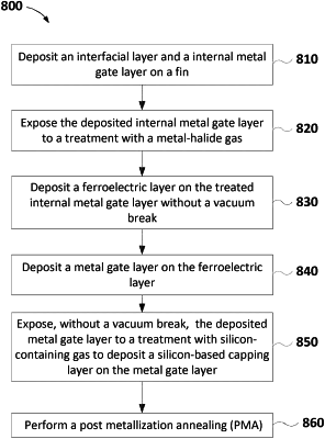
1. A method, comprising:
depositing an interfacial oxide layer on a fin structure;
depositing a first metal gate layer on the interfacial oxide layer;
performing a first in-situ process, comprising:
treating the first metal gate layer with a metal halide gas, and
depositing a ferroelectric layer on the treated first metal gate layer;
performing a second in-situ process comprising:
depositing a second metal gate layer on the ferroelectric layer; and
forming a silicon-based capping layer on the second metal gate layer.