| CPC H01L 29/0847 (2013.01) [H01L 29/24 (2013.01); H01L 29/267 (2013.01); H01L 29/41733 (2013.01); H01L 29/41775 (2013.01); H01L 29/45 (2013.01); H01L 29/516 (2013.01); H01L 29/517 (2013.01); H01L 29/7869 (2013.01)] | 19 Claims |

|
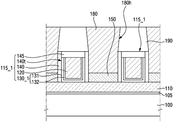
1. A semiconductor device comprising:
a substrate;
a metal oxide layer disposed on the substrate;
a gate structure disposed on the metal oxide layer, the gate structure including an insulating material layer and a gate electrode disposed on the insulating material layer, the insulating material layer including a ferroelectric material layer;
an interlayer insulating layer covering the gate structure and disposed on the metal oxide layer; and
a contact disposed in the interlayer insulating layer and connected to the metal oxide layer,
wherein the gate structure includes gate spacers defining a gate trench,
wherein the ferroelectric material layer extends along sidewalls and a bottom surface of the gate trench,
wherein a top surface of the ferroelectric material layer is lower than a top surface of the gate spacers, and
the contact is in direct contact with the gate spacers.
|