US 12,034,042 B2
Method of manufacturing multi-channel field effect transistors
Gyuhwan Ahn, Gunpo-si (KR); Sung Soo Kim, Hwaseong-si (KR); Chaeho Na, Changwon-si (KR); Woongsik Nam, Seoul (KR); and Donghyun Roh, Suwon-si (KR)
Assigned to Samsung Electronics Co., Ltd., Suwon-si (KR)
Filed by SAMSUNG ELECTRONICS CO., LTD., Suwon-si (KR)
Filed on Jul. 11, 2023, as Appl. No. 18/350,187.
Application 18/350,187 is a continuation of application No. 17/667,996, filed on Feb. 9, 2022, granted, now 11,735,626.
Application 17/667,996 is a continuation of application No. 16/903,015, filed on Jun. 16, 2020, granted, now 11,282,921, issued on Mar. 22, 2022.
Claims priority of application No. 10-2019-0130689 (KR), filed on Oct. 21, 2019.
Prior Publication US 2023/0352526 A1, Nov. 2, 2023
Int. Cl. H01L 29/06 (2006.01); H01L 21/02 (2006.01); H01L 21/762 (2006.01); H01L 21/8234 (2006.01); H01L 27/088 (2006.01); H01L 29/08 (2006.01); H01L 29/423 (2006.01); H01L 29/66 (2006.01); H01L 29/78 (2006.01); H01L 29/786 (2006.01)
CPC H01L 29/0653 (2013.01) [H01L 27/0886 (2013.01); H01L 29/0673 (2013.01); H01L 29/0847 (2013.01); H01L 29/42392 (2013.01); H01L 29/7851 (2013.01); H01L 29/78618 (2013.01); H01L 29/78696 (2013.01)] 12 Claims
OG exemplary drawing
 
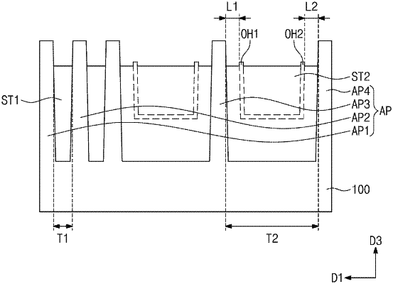
1. A method of manufacturing a semiconductor device, the method comprising:
forming a first trench and a second trench with active patterns therebetween on a substrate;
forming a first insulating layer on the first trench and the second trench;
forming a liner layer on the first insulating layer;
forming a second insulating layer on the liner layer; and
recessing the second insulating layer to form a first device isolation layer in the first trench and a second device isolation layer in the second trench,
wherein a width of the second trench in a first direction is greater than a width of the first trench in the first direction, and
wherein the second device isolation layer includes a first protrusion and a second protrusion which are formed by remaining portions of the liner layer.