| CPC H01L 28/65 (2013.01) [H01L 28/56 (2013.01); H01L 29/0847 (2013.01)] | 26 Claims |

|
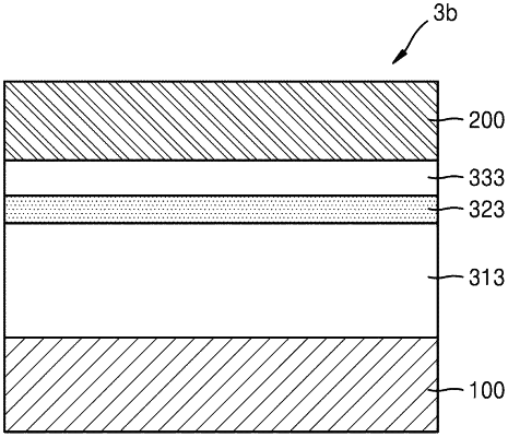
1. An electronic device comprising:
a lower electrode;
an upper electrode spaced apart from the lower electrode; and
a dielectric layer between the lower electrode and the upper electrode, the dielectric layer comprising
a first metal oxide region comprising a first metal oxide of one or more of Hf, Zr, Nb, Ta, Pr, Nd, Gd, Dy, Yb, Pb, Zn, Si, Ti, Sr, or Lu,
a second metal oxide region comprising a second metal oxide, the second metal oxide comprising one or more of Y, Sc, or Ce and further comprising one or more of Hf, Zr, Nb, Ta, Pr, Nd, Gd, Dy, Yb, Pb, Zn, Si, Ti, Sr, or Lu, and
a third metal oxide region comprising a third metal oxide of one or more of Al, Mg, or Be,
wherein a thickness of the second metal oxide is less than a thickness of the first metal oxide.
|