| CPC H01L 27/156 (2013.01) [H01L 33/0093 (2020.05); H01L 33/0095 (2013.01); H01L 33/007 (2013.01)] | 20 Claims |

|
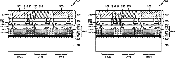
1. A micro light emitting diode (LED) display, comprising:
a support substrate;
a light emitting layer provided on the support substrate, the light emitting layer comprising:
a stacked structure including a first semiconductor layer, an active layer, and a second semiconductor layer;
a first electrode and a second electrode provided on a first side and a second side of the stacked structure, respectively; and
a plurality of light emitting regions each corresponding a pixel;
a bonding layer between the support substrate and the light emitting layer;
a drive layer provided on the light emitting layer and comprising a drive element, the drive element being electrically connected to the light emitting layer and configured to apply power to the plurality of light emitting regions of the light emitting layer; and
a color conversion layer including a plurality of color conversion regions for converting a light emitted from the light emitting layer into light colors,
wherein the support substrate is a separate substrate from a growth substrate on which the stacked structure of the light emitting layer is formed through a semiconductor deposition process, and the bonding layer is formed between the support substrate and the light emitting layer by bonding the support substrate to the growth substrate.
|