| CPC H01L 27/14636 (2013.01) [H01L 27/14618 (2013.01); H01L 27/14683 (2013.01)] | 17 Claims |

|
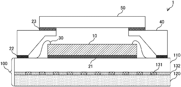
1. An imaging device, comprising:
an imaging element;
a substrate to which the imaging element is bonded, wherein:
the substrate is formed of an organic substrate and an inorganic substrate,
the organic substrate includes:
an insulation layer that is made of an organic material, and
a wiring layer made up of a material that has a low electric resistance,
the inorganic substrate includes:
an insulation layer that is made of an inorganic material, and
a plurality of wiring layers of a material having a melting point higher than a firing temperature of the inorganic material,
a thickness of each wiring layer of the plurality of wiring layers of the inorganic substrate is greater than a thickness of the wiring layer of the organic substrate, and
a thermal expansion coefficient of the inorganic substrate is lower than a thermal expansion coefficient of the organic substrate; and
a connection portion that connects the substrate and the imaging element.
|