| CPC H01L 27/1463 (2013.01) [H01L 27/14621 (2013.01); H01L 27/14627 (2013.01); H01L 27/1464 (2013.01); H01L 27/14645 (2013.01); H01L 27/14683 (2013.01)] | 20 Claims |
|
1. An image sensor, comprising:
a substrate including a first surface and a second surface, the first surface and the second surface being spaced apart from each other in a first direction;
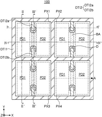
pixel regions in the substrate, the pixel regions being arranged in a direction parallel to the first surface;
a first photodiode and a second photodiode in the substrate, the first photodiode and the second photodiode corresponding to each of the pixel regions and being isolated from each other in a second direction perpendicular to the first direction;
a first device isolation film between the pixel regions;
a pair of second device isolation films between the first photodiode and the second photodiode in at least one of the pixel regions, the pair of second device isolation films extending from the first device isolation film to a region between the first photodiode and the second photodiode in a third direction perpendicular to the first direction and the second direction;
a doped layer in the substrate and having portions adjacent to respective second device isolation films of the pair of second device isolation films, the doped layer including impurities and extending in the first direction from the second surface of the substrate to a predetermined depth spaced apart from the first surface of the substrate, and the doped layer being isolated from the first device isolation film in the third direction; and
a barrier area between the pair of second device isolation films and between the portions of the doped layer, the barrier area having an electric potential greater than an electric potential of a portion of the substrate adjacent to the barrier area, wherein the barrier area includes the same impurities as the doped layer, which impurities are diffused from the doped layer.
|