| CPC H01L 27/1463 (2013.01) [H01L 27/14603 (2013.01); H01L 27/14623 (2013.01); H01L 27/1464 (2013.01)] | 20 Claims |
|
1. A semiconductor device comprising:
a substrate;
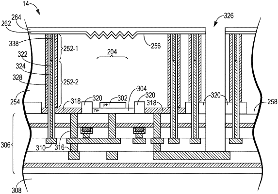
a single-photon avalanche diode formed in the substrate; and
a front side deep trench isolation structure in the substrate that is interposed between the single-photon avalanche diode and an adjacent single-photon avalanche diode, wherein the front side deep trench isolation structure comprises a metal filler in a trench, wherein the trench has a p-type doped semiconductor liner, wherein the p-type doped semiconductor liner has a first doping concentration in a first portion of the front side deep trench isolation structure and a second doping concentration that is different than the first doping concentration in a second portion of the front side deep trench isolation structure.
|