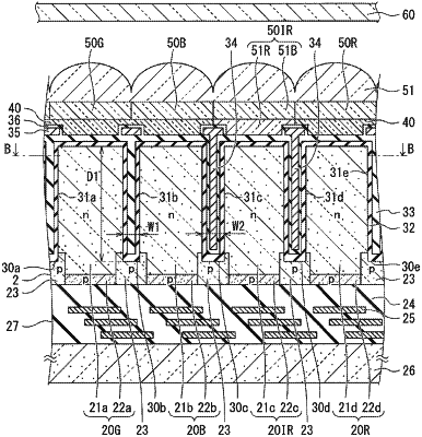
| CPC H01L 27/1463 (2013.01) [G02B 5/201 (2013.01); G02B 5/208 (2013.01); H01L 27/14607 (2013.01); H01L 27/14621 (2013.01); H01L 27/14623 (2013.01); H01L 27/14627 (2013.01); H01L 27/1464 (2013.01); H01L 27/14645 (2013.01); H01L 27/14649 (2013.01)] | 12 Claims |

|
1. A solid-state imaging device, comprising:
a substrate;
a first photoelectric conversion unit formed on the substrate;
a second photoelectric conversion unit that is formed on the substrate and adjacent to the first photoelectric conversion unit;
a third photoelectric conversion unit that is formed on the substrate and adjacent to the second photoelectric conversion unit;
infrared absorbing filters selectively disposed on a light incident surface side of the first photoelectric conversion unit and the second photoelectric conversion unit;
a first color filter disposed on the light incident surface side of the first photoelectric conversion unit;
a second color filter disposed on the light incident surface side of the second photoelectric conversion unit;
a third color filter disposed on the light incident surface side of the third photoelectric conversion unit;
a first element isolation unit disposed between the first photoelectric conversion unit and the second photoelectric conversion unit; and
a second element isolation unit disposed between the second photoelectric conversion unit and the third photoelectric conversion unit, wherein
a cross-sectional area of the first element isolation unit along a direction in which the first photoelectric conversion unit and the second photoelectric conversion unit are aligned is smaller than a cross-sectional area of the second element isolation unit along a direction in which the second photoelectric conversion unit and the third photoelectric conversion unit are aligned.
|