| CPC H01L 27/14627 (2013.01) [H01L 27/14643 (2013.01); H01L 27/14689 (2013.01); H01L 31/107 (2013.01)] | 19 Claims |

|
1. A semiconductor device, comprising:
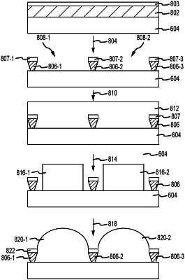
a plurality of single-photon avalanche diode pixels, wherein each of the single-photon avalanche diode pixels has an active region and an inactive region;
a plurality of microlenses comprising microlens material, wherein each of the microlenses covers the active region of a respective one of the single-photon avalanche diode pixels;
a containment grid that covers the inactive regions of the single-photon avalanche diode pixels, wherein portions of the containment grid are interposed between adjacent microlenses of the plurality of microlenses, and wherein the portions of the containment grid each have a tapered shape between the microlenses; and
material that is phyllic to the microlens material on the containment grid.
|