| CPC H01L 27/14605 (2013.01) [H01L 27/14607 (2013.01); H01L 27/1463 (2013.01); H01L 27/14632 (2013.01); H01L 27/14634 (2013.01); H01L 27/14687 (2013.01); H01L 27/1469 (2013.01); H04N 23/745 (2023.01); H04N 25/57 (2023.01); H04N 25/585 (2023.01); H04N 25/589 (2023.01); H04N 25/65 (2023.01); H04N 25/702 (2023.01); H04N 25/75 (2023.01); H04N 25/76 (2023.01); H04N 25/771 (2023.01); H04N 25/79 (2023.01); H01L 23/38 (2013.01); H01L 25/167 (2013.01); H01L 27/14621 (2013.01); H01L 27/14627 (2013.01); H01L 27/14636 (2013.01); H01L 27/1464 (2013.01); H01L 27/14645 (2013.01); H01L 31/024 (2013.01)] | 20 Claims |
|
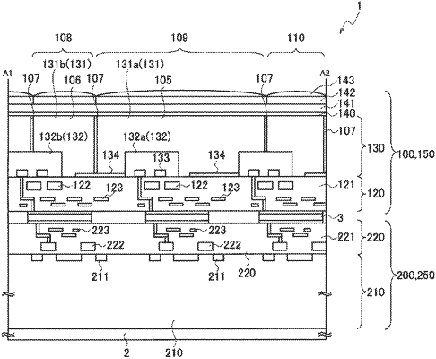
1. An imaging device comprising:
a first substrate including a first pixel circuit, the first pixel circuit includes a photodiode, a transfer transistor and a floating diffusion; and
a second substrate including a second pixel circuit connected to the first pixel circuit through a connection portion and configured to receive a potential change of the floating diffusion,
wherein the second pixel circuit includes
a first storage configured to store a first signal corresponding to the potential change generated by a first optical charge obtained by the photodiode during a first exposure time,
a second storage configured to store a second signal corresponding to the potential change generated by a second optical charge obtained by the photodiode during a second exposure time shorter than the first exposure time, and
a processing circuit configured to output a first image signal based on both of the first signal and the second signal in response to a voltage value corresponding to the first signal being equal to or greater than a predetermined value.
|