| CPC H01L 27/1244 (2013.01) [G02F 1/136286 (2013.01); G02F 1/13625 (2021.01); G02F 1/136295 (2021.01); G02F 1/1368 (2013.01); H01L 27/1288 (2013.01)] | 16 Claims |

|
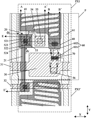
1. An array substrate, comprising:
a base substrate;
at least one first electrode arranged on the base substrate;
a gate line arranged on the base substrate, wherein the gate line is electrically insulated from the first electrode; and
at least one second electrode arranged on a side of the gate line away from the base substrate,
wherein at least one sub-pixel unit is provided on the base substrate, and the at least one sub-pixel unit comprises at least one first sub-pixel unit,
wherein the at least one first sub-pixel unit comprises:
a first connection portion arranged in a same layer as the second electrode and a second connection portion arranged in a same layer as the gate line, the second connection portion being electrically connected to the first electrode, and an orthographic projection of the second connection portion on the base substrate at least partially overlapping an orthographic projection of the first connection portion on the base substrate; and
a sixth connection portion arranged in a same layer as the first electrode, an orthographic projection of the sixth connection portion on the base substrate falling within an orthographic projection of the gate line on the base substrate,
wherein the array substrate further comprises:
a source and drain layer located on the side of the gate line away from the base substrate and located on a side of the second electrode facing the base substrate; and
a data line arranged in a same layer as the source and drain layer, wherein the data line extends in a first direction;
wherein the data line is provided with a data line widening portion having a width greater than a width of a part of the data line adjacent to the data line widening portion, and
wherein the array substrate further comprises a gate portion in the gate line and a first electrode bridge line arranged in the same layer as the gate line, wherein the first electrode bridge line and the gate line extend in a second direction intersecting the first direction, the first electrode bridge line is configured to electrically connect first electrodes in adjacent sub-pixels in the second direction, and an orthographic projection of the data line widening portion on the base substrate is located between the orthographic projection of the gate line on the base substrate and an orthographic projection of the first electrode bridge line on the base substrate.
|