| CPC H01L 27/124 (2013.01) [H01L 27/1222 (2013.01); H01L 27/1225 (2013.01); H01L 27/1237 (2013.01); H01L 27/127 (2013.01); H01L 29/7869 (2013.01); H01L 29/78696 (2013.01)] | 12 Claims |

|
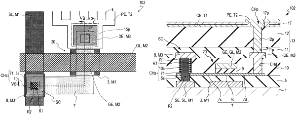
1. An active matrix substrate includes pixel regions, the active matrix substrate comprising:
a substrate;
a first conductive film supported on a main surface of the substrate;
a lower insulating layer covers the first conductive film;
an oxide semiconductor layer located above the lower insulating layer;
a gate insulating layer on the oxide semiconductor layer;
a second conductive film on the gate insulating layer;
an interlayer insulating layer covers the second conductive film;
a third conductive film located above the interlayer insulating layer;
a lower opening provided in the lower insulating layer;
a first opening provided in the interlayer insulating layer;
oxide semiconductor TFTs provided in association with the pixel regions; wherein
at least one of the oxide semiconductor TFTs includes:
the oxide semiconductor layer including a channel region, and a first region and a second region located on respective sides of the channel region;
a gate electrode made of the second conductive film, and overlapping the channel region of the oxide semiconductor layer; and
a source electrode made of the first conductive film, and electrically connected to the first region via a connection portion;
the connection portion includes a first connection region where a connection electrode made of the third conductive film and the first region are electrically connected, and a second connection region where the connection electrode and the source electrode are electrically connected; and
the second connection region is arranged within the lower opening and the first opening.
|