| CPC H01L 27/0605 (2013.01) [H01L 21/8213 (2013.01); H01L 27/0629 (2013.01); H01L 29/0615 (2013.01); H01L 29/0623 (2013.01); H01L 29/1095 (2013.01); H01L 29/1608 (2013.01); H01L 29/36 (2013.01); H01L 29/41741 (2013.01); H01L 29/66068 (2013.01); H01L 29/7806 (2013.01); H01L 29/7811 (2013.01); H01L 29/7813 (2013.01)] | 20 Claims |
|
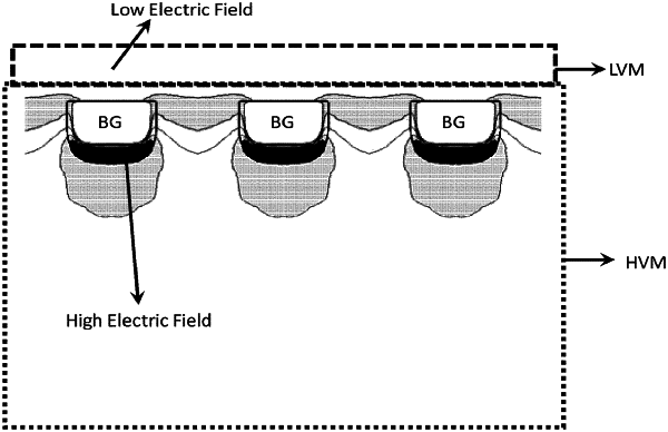
1. A power device, comprising:
a high voltage module comprising:
a substrate having a first conductivity type;
a first drift layer on the substrate, the first drift layer having one of (i) a same conductivity type as the substrate and (ii) an opposite conductivity type as the substrate;
a buried grid on the first drift layer, the buried grid having a conductivity type opposite to the conductivity type of the first drift layer; and
a second drift layer on the first drift layer and the buried grid, the second drift layer having conductivity type of a same conductivity type as the first drift layer; and
a low voltage module in electrical contact with the high voltage module, the low voltage module having at least one low voltage device with a blocking voltage less than a blocking voltage of the high voltage module,
wherein the at least one low voltage device has at least one other epitaxial layer as a common layer with the high voltage module.
|