| CPC H01L 25/167 (2013.01) [H01L 24/32 (2013.01); H01L 24/83 (2013.01); H01L 24/98 (2013.01); H01L 27/1262 (2013.01); H01L 33/62 (2013.01); H01L 2224/32145 (2013.01); H01L 2224/83005 (2013.01); H01L 2224/83048 (2013.01); H01L 2224/838 (2013.01); H01L 2924/12041 (2013.01); H01L 2933/0066 (2013.01)] | 14 Claims |

|
1. A display panel, comprising:
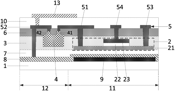
a base substrate provided with a circuit area and a light-emitting area;
a driving circuit in the circuit area of the base substrate;
an organic insulating layer covering the light-emitting area of the base substrate;
a light-emitting element embedded in the organic insulating layer, wherein an overlap area between an orthographic projection of the light-emitting element on the base substrate and an orthographic projection of the driving circuit on the base substrate is 0, and the light-emitting element comprises a bottom surface facing the base substrate, a top surface facing away from the base substrate, and side surfaces between the bottom surface and the top surface; wherein the bottom surface and the side surfaces are in direct contact with the organic insulating layer, the light-emitting element is provided with a first electrode at a side, facing away from the base substrate, of the light-emitting element;
a first lapping electrode on the side, facing away from the base substrate, of the light-emitting element, wherein the light-emitting element is electrically connected to the driving circuit through the first lapping electrode; and
an interlayer insulating layer between a film layer in which the first lapping electrode is located and the light-emitting element, wherein the interlayer insulating layer is in direct contact with the top surface and is made of an inorganic material;
wherein the organic insulating layer further covers the circuit area; and
the driving circuit comprises an active layer, a gate insulating layer and a gate sequentially stacked on the base substrate, and wherein
the light-emitting element is electrically connected to the first lapping electrode through at least one first via hole penetrating through the interlayer insulating layer;
the first lapping electrode is electrically connected to the active layer through a second via hole penetrating through the interlayer insulating layer and the organic insulating layer;
a position at which the first electrode is electrically connected to the first lapping electrode is external to the organic insulating layer; and
the organic insulating layer, which is in direct contact with the bottom surface and the side surfaces and through which the second via hole penetrates, is a continuously distributed single film made of a same organic material.
|
|
9. A preparation method of the display panel of claim 1, comprising:
forming the driving circuit in the circuit area of the base substrate;
forming the organic insulating layer covering the light-emitting area on the base substrate;
adhering the light-emitting element to a box alignment substrate through pyrolysis adhesives;
aligning and bonding the box alignment substrate with the light-emitting element and the base substrate on which the organic insulating layer is formed through an aligning device, to embed the light-emitting element within the organic insulating layer; wherein the overlap area between the orthographic projection of the light-emitting element on the base substrate and the orthographic projection of the driving circuit on the base substrate is 0;
peeling off the pyrolysis adhesives; and
forming the first lapping electrode on the side, facing away from the base substrate, of the light-emitting element; wherein the light-emitting element is electrically connected to the driving circuit through the first lapping electrode.
|