| CPC H01L 25/105 (2013.01) [G11C 5/025 (2013.01); G11C 5/04 (2013.01); H01L 24/19 (2013.01); H01L 24/20 (2013.01); H01L 25/50 (2013.01); H01L 24/13 (2013.01); H01L 24/48 (2013.01); H01L 2224/04105 (2013.01); H01L 2224/12105 (2013.01); H01L 2224/13111 (2013.01); H01L 2224/16225 (2013.01); H01L 2224/32145 (2013.01); H01L 2224/32225 (2013.01); H01L 2224/48091 (2013.01); H01L 2224/48227 (2013.01); H01L 2224/73265 (2013.01); H01L 2225/1023 (2013.01); H01L 2225/1035 (2013.01); H01L 2225/1041 (2013.01); H01L 2225/1058 (2013.01); H01L 2924/00014 (2013.01); H01L 2924/14 (2013.01); H01L 2924/1434 (2013.01); H01L 2924/15311 (2013.01); H01L 2924/15331 (2013.01); H01L 2924/181 (2013.01)] | 20 Claims |

|
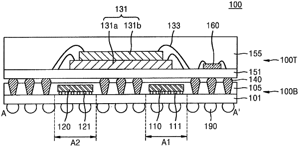
1. A package-on-package (PoP) semiconductor package, comprising:
an upper package; and
a lower package, the lower package including:
a first semiconductor device in a first area;
a second semiconductor device in a second area; and
a command-and-address (CA) vertical interconnection, a data input-output vertical interconnection, a memory management vertical interconnection, a power vertical interconnection, and a ground vertical interconnection,
wherein the CA vertical interconnection, the data input-output vertical interconnection, the memory management vertical interconnection, the power vertical interconnection, and the ground vertical interconnection are adjacent to the first semiconductor device at a same vertical level,
wherein the CA vertical interconnection, the data input-output vertical interconnection, the memory management vertical interconnection, the power vertical interconnection, and the ground vertical interconnection are laterally spaced apart from the first semiconductor device, and
wherein the power vertical interconnection and the ground vertical interconnection are not between the first semiconductor device and the second semiconductor device.
|