| CPC H01L 25/0753 (2013.01) [H01L 27/1207 (2013.01); H01L 27/1225 (2013.01); H01L 29/78648 (2013.01); H01L 29/7869 (2013.01); H01L 33/62 (2013.01)] | 20 Claims |

|
1. A display device comprising:
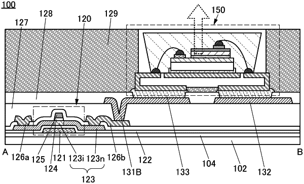
a pixel comprising a first transistor, a second transistor, a first conductive layer and a light-emitting diode package over the first conductive layer,
wherein the light-emitting diode package comprises a case, a first light-emitting diode, a second light-emitting diode, an adhesive layer, a second conductive layer, a third conductive layer and a fourth conductive layer,
wherein the first light-emitting diode and the second light-emitting diode are sealed in the case,
wherein the first light-emitting diode comprises a first electrode and a second electrode,
wherein the second light-emitting diode comprises a third electrode and a fourth electrode,
wherein the adhesive layer has conductivity,
wherein one of a source and a drain of the first transistor is electrically connected to the first electrode through the second conductive layer,
wherein one of a source and a drain of the second transistor is electrically connected to the third electrode through the third conductive layer,
wherein the first conductive layer is electrically connected to the second electrode through the fourth conductive layer,
wherein the first conductive layer is electrically connected to the fourth electrode through the fourth conductive layer, and
wherein a constant potential is supplied to the first conductive layer.
|