| CPC H01L 25/0753 (2013.01) [H01L 33/62 (2013.01); H01L 2933/0066 (2013.01)] | 18 Claims |

|
1. A light emitting device comprising:
a substrate including a plurality of emission areas;
a first electrode disposed on the substrate;
a second electrode disposed on the substrate and spaced apart from the first electrode;
a plurality of light emitting elements disposed on the substrate, each of the plurality of light emitting elements including a first end and a second end in a longitudinal direction of the plurality of light emitting elements;
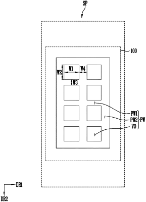
a bank disposed in each of the plurality of emission areas, having a mesh shape in a plan view, and including a plurality of openings in which portions of the plurality of emission areas are exposed;
a first contact electrode that electrically connects the first electrode with the first end of each of the plurality of light emitting elements; and
a second contact electrode that electrically connects the second electrode with the second end of each of the plurality of light emitting elements,
wherein at least one of the plurality of light emitting elements is disposed in each of the openings.
|