| CPC H01L 25/0753 (2013.01) [H01R 12/57 (2013.01); H05K 1/181 (2013.01); H05K 2201/10106 (2013.01); H05K 2201/10189 (2013.01); H05K 2201/2009 (2013.01)] | 13 Claims |

|
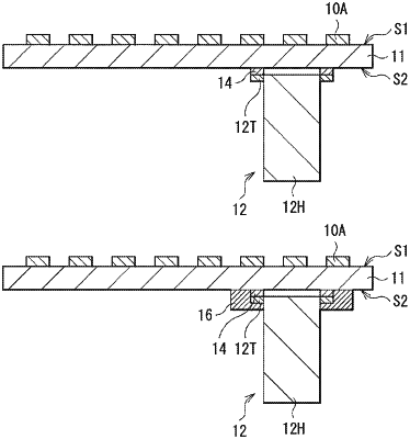
1. A display unit, comprising:
a substrate that includes a first surface and a second surface opposed to the first surface;
a plurality of light emitting devices on the first surface of the substrate;
a mounting member in a selective region of the second surface of the substrate;
a base opposed to the substrate, wherein
the base includes an opening,
the mounting member is inserted through the opening of the base, and
the opening includes a gap between a periphery edge of the opening and the mounting member; and
a rigid member in the gap of the opening, wherein the rigid member is in contact with the base and the mounting member.
|