| CPC H01L 25/0652 (2013.01) [H01L 25/18 (2013.01); H01L 25/50 (2013.01); H01L 2225/06506 (2013.01); H01L 2225/06527 (2013.01); H01L 2225/06562 (2013.01)] | 20 Claims |

|
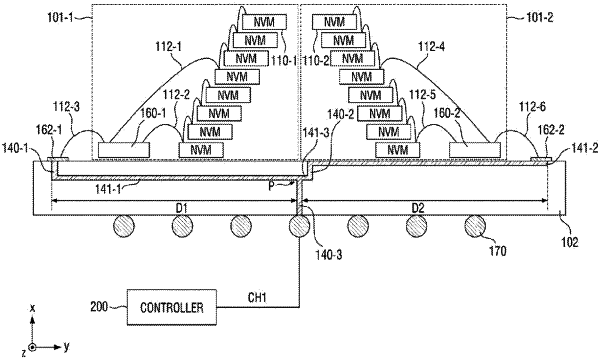
1. A semiconductor package comprising:
a substrate;
a first buffer pad and a second buffer pad located on an upper part of the substrate;
a first buffer chip and a second buffer chip electrically connected to each of the first buffer pad and the second buffer pad;
a plurality of nonvolatile memory chips located on the upper part of the substrate and including a first nonvolatile memory chip and a second nonvolatile memory chip, the first nonvolatile memory chip being electrically connected to the first buffer chip, and the second nonvolatile memory chip being electrically connected to the second buffer chip;
a plurality of external connection terminals connected to a lower part of the substrate; and
a rewiring pattern located inside the substrate, the rewiring pattern configured to diverge an external electric signal received through one of the plurality of external connection terminals into first and second signals, transmit the first signal to the first buffer chip and transmit the second signal to the second buffer chip,
wherein the first buffer pad comprises a first_first I/O pad and a second_first I/O pad connecting the first buffer chip and the second buffer pad comprises a first second I/O pad and a second_second I/O pad connecting the second buffer chip,
wherein the rewiring pattern comprises a first rewiring pattern connecting the first_first I/O pad and the first second I/O pad and a second rewiring pattern connecting the second_first I/O pad and the second_second I/O pad,
wherein the external electric signal is diverged into the first and second signals at a plurality of diverging points in the rewiring pattern,
the diverging points comprise a first diverging point at which the external electric signal is diverged into the first and second buffer chips in the first rewiring pattern and a second diverging point at which the external electric signal is diverged into the first and second buffer chips in the second rewiring pattern, and
from a planar perspective, the first and second diverging points are spaced apart from each other in a direction parallel to the upper surface of the substrate.
|