| CPC H01L 24/48 (2013.01) [H01L 21/02164 (2013.01); H01L 21/0217 (2013.01); H01L 21/02288 (2013.01); H01L 23/293 (2013.01); H01L 23/3135 (2013.01); H01L 23/3142 (2013.01); H01L 23/4952 (2013.01); H01L 23/49582 (2013.01); H01L 24/03 (2013.01); H01L 24/05 (2013.01); H01L 24/45 (2013.01); H01L 24/83 (2013.01); H01L 24/85 (2013.01); H01L 21/02266 (2013.01); H01L 21/02271 (2013.01); H01L 21/02274 (2013.01); H01L 21/0228 (2013.01); H01L 23/3107 (2013.01); H01L 24/29 (2013.01); H01L 24/32 (2013.01); H01L 24/73 (2013.01); H01L 2224/0346 (2013.01); H01L 2224/03826 (2013.01); H01L 2224/03827 (2013.01); H01L 2224/03831 (2013.01); H01L 2224/04042 (2013.01); H01L 2224/05073 (2013.01); H01L 2224/05139 (2013.01); H01L 2224/05147 (2013.01); H01L 2224/05624 (2013.01); H01L 2224/05639 (2013.01); H01L 2224/05644 (2013.01); H01L 2224/05647 (2013.01); H01L 2224/05655 (2013.01); H01L 2224/05657 (2013.01); H01L 2224/05664 (2013.01); H01L 2224/05666 (2013.01); H01L 2224/05681 (2013.01); H01L 2224/05684 (2013.01); H01L 2224/2919 (2013.01); H01L 2224/32245 (2013.01); H01L 2224/45139 (2013.01); H01L 2224/45144 (2013.01); H01L 2224/45147 (2013.01); H01L 2224/45565 (2013.01); H01L 2224/45572 (2013.01); H01L 2224/45573 (2013.01); H01L 2224/45611 (2013.01); H01L 2224/45618 (2013.01); H01L 2224/45639 (2013.01); H01L 2224/45644 (2013.01); H01L 2224/45649 (2013.01); H01L 2224/45655 (2013.01); H01L 2224/45657 (2013.01); H01L 2224/45664 (2013.01); H01L 2224/45666 (2013.01); H01L 2224/4567 (2013.01); H01L 2224/45671 (2013.01); H01L 2224/45672 (2013.01); H01L 2224/4568 (2013.01); H01L 2224/45686 (2013.01); H01L 2224/4569 (2013.01); H01L 2224/45693 (2013.01); H01L 2224/48091 (2013.01); H01L 2224/48106 (2013.01); H01L 2224/4813 (2013.01); H01L 2224/48247 (2013.01); H01L 2224/4846 (2013.01); H01L 2224/48463 (2013.01); H01L 2224/48465 (2013.01); H01L 2224/4847 (2013.01); H01L 2224/48507 (2013.01); H01L 2224/73265 (2013.01); H01L 2224/85205 (2013.01); H01L 2224/85375 (2013.01); H01L 2224/85801 (2013.01); H01L 2224/8592 (2013.01); H01L 2924/00014 (2013.01); H01L 2924/0132 (2013.01); H01L 2924/10253 (2013.01); H01L 2924/181 (2013.01)] | 12 Claims |
|
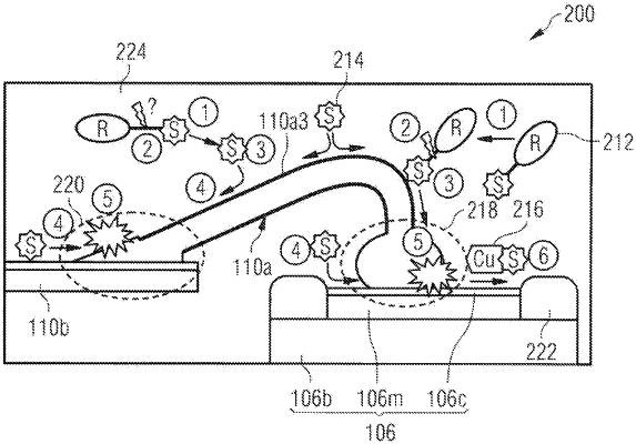
1. A method of forming an electrical contact, comprising:
depositing, by atomic layer deposition, a non-conductive layer over at least a region of a metal surface; and
after depositing, by atomic layer deposition, of the non-conductive layer over the at least a region of the metal surface, electrically contacting a region of the non-conductive layer with a metal contact structure,
wherein the non-conductive layer comprises at least one material of a group of materials comprising aluminum oxide, aluminum nitride, silicon oxide, and/or silicon nitride materials; and
wherein the metal contact structure comprises at least one metal of a group of metals comprising copper, silver, gold, palladium, and/or alloys thereof.
|