| CPC H01L 24/13 (2013.01) [H01L 21/563 (2013.01); H01L 23/3128 (2013.01); H01L 23/3185 (2013.01); H01L 23/49816 (2013.01); H01L 24/11 (2013.01); H01L 24/14 (2013.01); H01L 24/16 (2013.01); H01L 24/17 (2013.01); H01L 24/81 (2013.01); H01L 25/0652 (2013.01); H01L 25/0657 (2013.01); H01L 2224/11464 (2013.01); H01L 2224/13026 (2013.01); H01L 2224/13083 (2013.01); H01L 2224/13147 (2013.01); H01L 2224/13155 (2013.01); H01L 2224/16013 (2013.01); H01L 2224/16227 (2013.01); H01L 2924/181 (2013.01)] | 20 Claims |
|
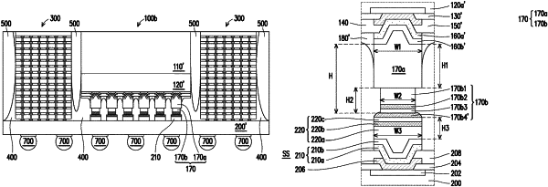
1. A package structure, comprising:
a substrate;
a semiconductor die disposed over the substrate;
a first conductive bump disposed on and electrically connected to the semiconductor die, wherein a first width of a first end of the first conductive bump is greater than a second width of a second end of the first conductive bump, and the first end is opposite to the second end; and
a memory device disposed on and electrically connected to the substrate, wherein a first distance between the semiconductor die and the substrate is greater than a second distance between the memory device and the substrate, wherein the substrate comprises second conductive bumps, a third width of the second conductive bumps is greater than the second width of the second end, and the third width of the second conductive bumps is substantially equal to the first width of the first end.
|