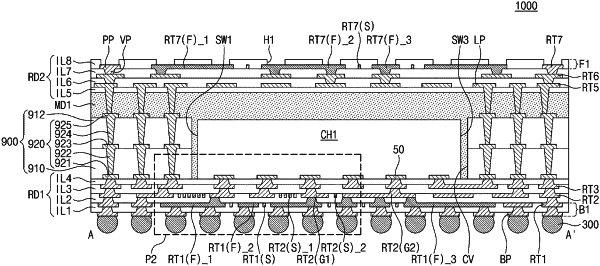
| CPC H01L 23/562 (2013.01) [H01L 23/3128 (2013.01); H01L 23/49811 (2013.01); H01L 23/49822 (2013.01); H01L 23/49838 (2013.01); H01L 24/08 (2013.01); H01L 2224/08235 (2013.01)] | 20 Claims |

|
1. A semiconductor package, comprising:
a first redistribution substrate;
a semiconductor device disposed on the first redistribution substrate and having a first sidewall; and
a mold layer that covers the semiconductor device and the first redistribution substrate,
wherein the first redistribution substrate includes:
a first redistribution dielectric layer;
a first reinforcement pattern at the first redistribution dielectric layer, the first reinforcement pattern overlapping the semiconductor device and the mold layer; and
a first bonding pad and a second bonding pad, each of the first bonding pad and the second bonding pad penetrating the first redistribution dielectric layer and contacting the first reinforcement pattern,
wherein the second bonding pad is spaced apart from the first bonding pad in a first direction,
wherein, when viewed in a plan view, the first sidewall extends in a second direction between the first bonding pad and the second bonding pad,
wherein the first bonding pad has a first width in a second direction orthogonal to the first direction, and
wherein, when viewed in the plan view, the first reinforcement pattern overlaps the first sidewall of the semiconductor device and has a second width in the second direction, the second width being greater than the first width.
|