| CPC H01L 23/5283 (2013.01) [H01L 21/311 (2013.01); H01L 21/76816 (2013.01); H01L 21/76877 (2013.01); H01L 21/76895 (2013.01); H01L 23/5226 (2013.01); H01L 23/535 (2013.01); H10B 41/10 (2023.02); H10B 41/27 (2023.02); H10B 43/10 (2023.02); H10B 43/27 (2023.02); H10B 43/40 (2023.02); H10B 43/50 (2023.02)] | 20 Claims |

|
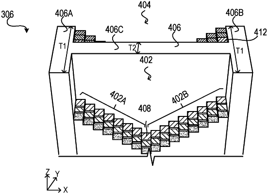
1. A method for fabricating a semiconductor device, comprising:
forming an initial stack of sacrificial word line layers and insulating layers that are disposed alternately over a substrate of the semiconductor device;
forming a first staircase in a first staircase region of a connection region of the initial stack, the first staircase having first stairs and second stairs; and
forming a second staircase in a second staircase region of the connection region of the initial stack, wherein:
the connection region of the initial stack comprises a separation region between the first and second staircases,
the connection region is positioned between array regions at opposing sides of the initial stack, and
each of the first stairs and the second stairs corresponds to one of the sacrificial word line layers, the sacrificial word line layers corresponding to the first stairs being a different set of sacrificial word line layers than the sacrificial word line layers corresponding to the second stairs and the corresponding sacrificial word line layer of a lowest stair in the first stairs is a different sacrificial word line layer than the corresponding sacrificial word line layer of a lowest stair in the second stairs.
|