| CPC H01L 23/5256 (2013.01) [H01L 21/76886 (2013.01); H01L 27/0255 (2013.01); H01L 27/0629 (2013.01); H01L 27/088 (2013.01); H01L 29/868 (2013.01)] | 18 Claims |

|
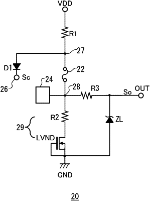
1. A trimming circuit comprising:
a body portion configured to output a voltage according to a presence or absence of disconnection of a fuse resistor, the body portion including:
a fuse resistor formed by a polysilicon layer arranged on a semiconductor substrate via an insulating film;
a pad for trimming connected to one end of the fuse resistor;
an output terminal electrically connected to a connection point between the fuse resistor and the pad, and configured to output a voltage according to the presence or absence of disconnection of the fuse resistor; and
a diode formed on the semiconductor substrate, having one end connected to another end of the fuse resistor;
a second resistance portion having one end connected to the connection point between the fuse resistor and the pad, and another end connected to second potential; and
a protection diode connected between the other end of the second resistance portion and the output terminal.
|