| CPC H01L 23/49838 (2013.01) [H01L 21/485 (2013.01); H01L 23/49827 (2013.01)] | 18 Claims |
|
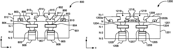
1. An integrated circuit (IC) package substrate, comprising:
a metallization level within a dielectric material, wherein the metallization level comprises a plurality of conductive features each having a top surface and a sidewall surface,
wherein the top surface of a first conductive feature of the plurality of conductive features has a first average surface roughness and the sidewall surface of a second conductive feature of the plurality of conductive features has a second average surface roughness that is less than the first average surface roughness,
wherein the sidewall surface of the first conductive feature has a third average surface roughness that is greater than the second average surface roughness and the top surface of the second conductive feature has a fourth average surface roughness that is less than the first average surface roughness,
wherein the second conductive feature comprises a first material, and wherein a second material is over the top surface and the sidewall surface of the second conductive feature.
|