| CPC H01L 23/49827 (2013.01) [H01L 21/4853 (2013.01); H01L 21/486 (2013.01); H01L 23/13 (2013.01); H01L 23/49838 (2013.01); H01L 24/17 (2013.01); H01L 24/81 (2013.01); H01L 25/0652 (2013.01); H01L 25/0657 (2013.01); H01L 25/105 (2013.01); H01L 25/18 (2013.01); H01L 25/50 (2013.01); H01L 23/3128 (2013.01); H01L 23/49811 (2013.01); H01L 24/13 (2013.01); H01L 24/16 (2013.01); H01L 24/48 (2013.01); H01L 25/0655 (2013.01); H01L 2224/131 (2013.01); H01L 2224/1413 (2013.01); H01L 2224/14179 (2013.01); H01L 2224/16145 (2013.01); H01L 2224/16225 (2013.01); H01L 2224/16227 (2013.01); H01L 2224/45099 (2013.01); H01L 2224/48145 (2013.01); H01L 2224/48227 (2013.01); H01L 2225/06517 (2013.01); H01L 2225/0652 (2013.01); H01L 2225/06548 (2013.01); H01L 2225/06572 (2013.01); H01L 2225/06586 (2013.01); H01L 2225/1023 (2013.01); H01L 2225/1058 (2013.01); H01L 2924/00014 (2013.01); H01L 2924/01029 (2013.01); H01L 2924/1434 (2013.01); H01L 2924/1436 (2013.01); H01L 2924/1437 (2013.01); H01L 2924/1438 (2013.01); H01L 2924/15153 (2013.01); H01L 2924/15311 (2013.01); H01L 2924/15321 (2013.01); H01L 2924/15331 (2013.01); H01L 2924/181 (2013.01)] | 16 Claims |
|
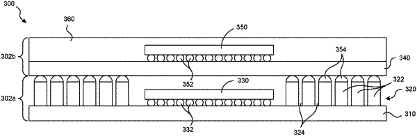
1. A package-on-package system, comprising:
a first semiconductor device package including:
a base substrate including a first side having a die-attach region and a perimeter region;
a first semiconductor die attached to the die-attach region of the base substrate, wherein the first semiconductor die has a front side facing the first side of the base substrate and a backside opposite the front side and at a first height above the base substrate;
an interconnect array over the perimeter region of the base substrate, wherein the interconnect array comprises a plurality of interconnect structures, wherein each of the plurality of interconnect structures includes at least one vertical sidewall, and wherein the plurality of interconnect structures extends from the first side of the base substrate to a second height greater than the first height, and wherein each of the plurality of interconnect structures comprises a freestanding conductive post; and
a plurality of electrical couplers; and
a second semiconductor device package including:
an interposer substrate having a plurality of package terminals, wherein each individual package terminal is electrically coupled to a corresponding individual interconnect structure through a respective electrical coupler of the plurality of electrical couplers, and wherein the plurality of electrical couplers is separate from and below the interposer substrate; and
a second semiconductor die attached to the interposer substrate.
|