| CPC H01L 23/49816 (2013.01) [H01L 21/4853 (2013.01); H01L 21/76894 (2013.01); H01L 23/3135 (2013.01); H01L 23/49861 (2013.01); H01L 24/13 (2013.01); H01L 2021/60112 (2013.01); H01L 2224/13 (2013.01)] | 16 Claims |

|
1. A semiconductor device, comprising:
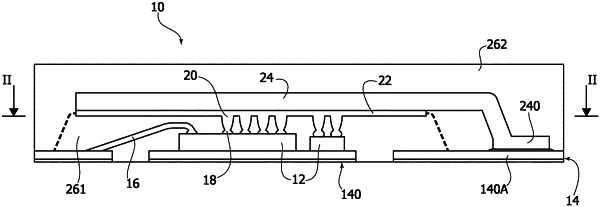
a leadframe including a die pad having at least one semiconductor chip mounted thereon and connection pads;
at least one portion of an insulating package over the at least one semiconductor chip on the leadframe, said at least one portion made of a laser direct structuring material molding on the at least one semiconductor chip, the at least one portion of the insulating package having an upper surface and a side surface from which said connection pads extend;
at least one electrically conductive formation comprising a paddle portion extending on the upper surface of the at least one portion of the insulating package and a via portion extending through an opening in the at least one portion of the insulating package to the at least one semiconductor chip; and
an electrically conductive clip applied onto an upper surface of the paddle portion and extending over both the upper surface and the side surface of the at least one portion of the insulating package, the electrically conductive clip in electrical and physical contact with the upper surface of the paddle portion and in electrical and physical contact with an upper surface of one or more connection pads of the leadframe, with the at least one semiconductor chip located intermediate the leadframe and the electrically conductive clip.
|