| CPC H01L 23/49537 (2013.01) [H01L 23/49575 (2013.01); H01L 25/072 (2013.01); H01L 25/162 (2013.01); H02M 1/08 (2013.01); H02M 7/537 (2013.01); H05K 1/181 (2013.01); H01L 23/3121 (2013.01); H01L 23/49513 (2013.01); H01L 24/32 (2013.01); H01L 24/37 (2013.01); H01L 24/40 (2013.01); H01L 24/48 (2013.01); H01L 24/73 (2013.01); H01L 2224/32245 (2013.01); H01L 2224/37147 (2013.01); H01L 2224/3716 (2013.01); H01L 2224/40175 (2013.01); H01L 2224/40499 (2013.01); H01L 2224/48245 (2013.01); H01L 2224/73221 (2013.01); H01L 2224/73263 (2013.01); H01L 2924/01029 (2013.01); H01L 2924/01047 (2013.01); H01L 2924/0105 (2013.01); H01L 2924/01082 (2013.01); H01L 2924/014 (2013.01); H01L 2924/10253 (2013.01); H01L 2924/10272 (2013.01); H01L 2924/13055 (2013.01); H01L 2924/13091 (2013.01); H01L 2924/1433 (2013.01); H02P 27/06 (2013.01); H05K 2201/10015 (2013.01); H05K 2201/10166 (2013.01)] | 12 Claims |

|
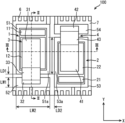
1. A semiconductor device configured to be mountable on a wiring board having wiring, the semiconductor device comprising:
a first semiconductor element having two electrodes respectively disposed on two surfaces of the first semiconductor element;
a second semiconductor element having two electrodes respectively disposed on two surfaces of the second semiconductor element;
two first terminals configured to be connected to a part of the wiring in a state of being mounted on the wiring board, electrically connected to the two electrodes of the first semiconductor element, respectively, and arranged side by side in one direction;
two second terminals configured to be connected to another part of the wiring in the state of being mounted on the wiring board, electrically connected to the two electrodes of the second semiconductor element, respectively, arranged side by side in the one direction to be adjacent to the two first terminals; and
a sealing resin portion covering the first semiconductor element, the second semiconductor element, the first terminals, and the second terminals in a state where facing surfaces of the first terminals and the second terminals are exposed from the sealing resin portion, the facing surfaces of the first terminals and the second terminals face the wiring board in the state of being mounted on the wiring board, wherein
the facing surfaces of the two first terminals have area ratios different from each other,
the facing surfaces of the two second terminals have area ratios different from each other, and
one of the first terminals is arranged adjacent to both the two second terminals.
|