| CPC H01L 22/12 (2013.01) [H01L 21/67253 (2013.01); H01L 21/681 (2013.01)] | 22 Claims |
|
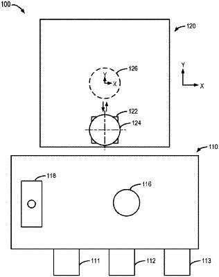
1. A device for measuring wafers, comprising:
a moving platform, for adjusting the location of wafers;
a first pre-alignment module and a first image recognition module, for aligning a first wafer at a first location on the moving platform before measuring the first wafer;
a second pre-alignment module and a second image recognition module, for aligning a second wafer at a second location on the moving platform before measuring the second wafer; and
a measurement module, for measuring the first wafer at a third location on the moving platform while the second wafer is being aligned at the second location on the moving platform and measuring the second wafer at the third location on the moving platform after measuring the first wafer;
wherein the first location, the second location and the third location are different from each other.
|