| CPC H01L 21/823842 (2013.01) [H01L 21/28088 (2013.01); H01L 21/28123 (2013.01); H01L 21/32134 (2013.01); H01L 21/823821 (2013.01); H01L 27/0924 (2013.01); H01L 29/4966 (2013.01)] | 20 Claims |
|
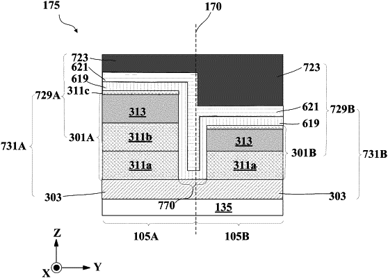
1. A method, comprising:
forming a gate dielectric layer on a first fin structure, a second fin structure, and an insulating layer between the first and second fin structures;
forming a first work function stack on the gate dielectric layer over the first fin structure and a first portion of the insulating layer;
forming a second work function stack on the gate dielectric layer over the second fin structure and a second portion of the insulating layer, wherein the second work function stack is in contact with the first work function stack; and
forming a conductive structure between the first work function stack and the second work function stack, wherein the conductive structure is in contact with the gate dielectric layer.
|