| CPC H01L 21/823431 (2013.01) [H01L 29/7842 (2013.01); H01L 29/7845 (2013.01); H01L 29/7846 (2013.01); H01L 29/785 (2013.01)] | 20 Claims |
|
1. An integrated circuit device structure, comprising:
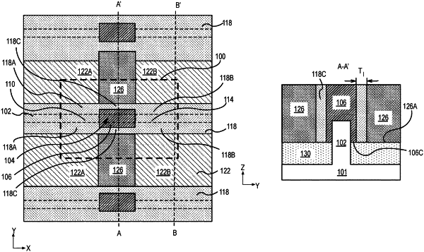
a first transistor structure comprising a first gate, a first source and a first drain coupled to a first fin;
a second transistor structure adjacent to the first transistor structure, wherein the second transistor comprises a second gate, a second source and a second drain coupled to a second fin, the second fin separated from the first fin by a space;
a material comprising a metal occupying the space between the first and second fins, and adjacent to a portion of each of the first and second transistor structures, wherein the material comprising the metal is between the first and second gates, between the first source and second sources, or between the first and second drains; and
a dielectric material within the space, the dielectric material between a sidewall of the material comprising the metal and a sidewall of each of the first and second transistor structures.
|