| CPC H01L 21/76871 (2013.01) [H01L 21/76805 (2013.01); H01L 21/7684 (2013.01); H01L 21/76843 (2013.01); H01L 21/76862 (2013.01); H01L 21/76889 (2013.01); H01L 21/76895 (2013.01); H01L 23/53266 (2013.01); H01L 23/535 (2013.01); H01L 29/66795 (2013.01); H01L 29/7851 (2013.01)] | 20 Claims |

|
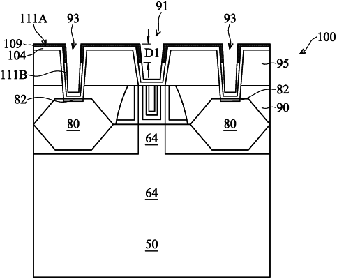
1. A method of forming a semiconductor device, the method comprising:
forming a dielectric layer over a conductive feature;
forming recess in the dielectric layer; and
forming a contact plug in the recess of the dielectric layer, forming the contact plug comprising:
forming a conductive layer along sidewalls of the recess, a first portion of the conductive layer proximal a bottom of the recess comprising a first concentration of a first impurity, a second portion of the conductive layer proximal a top of the recess comprising a second concentration of the first impurity, and wherein the second concentration of the first impurity is less than the first concentration of the first impurity, wherein the first impurity comprises oxygen or boron; and
forming a conductive material over the conductive layer.
|