| CPC H01L 21/76831 (2013.01) [H01L 21/76816 (2013.01); H01L 21/76834 (2013.01); H01L 21/76849 (2013.01); H01L 21/76877 (2013.01); H01L 21/76897 (2013.01); H01L 23/5226 (2013.01); H01L 23/528 (2013.01); H01L 23/53228 (2013.01); H01L 23/53238 (2013.01); H01L 21/76883 (2013.01)] | 19 Claims |

|
1. A semiconductor device, comprising:
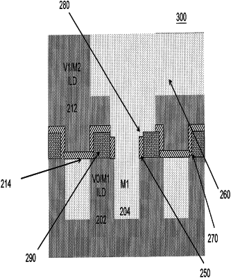
interconnect lines disposed adjacently in a first interlevel dielectric, ILD;
first ILD regions separating the interconnect lines, the first ILD regions comprising first ILD sidewalls that border the interconnect lines;
second ILD regions disposed directly on the first ILD regions, wherein:
second ILD sidewalls of second ILD regions are aligned to corresponding first ILD sidewalls of first ILD regions;
interfaces between the second ILD regions and corresponding underlying first ILD regions are substantially coplanar with upper surfaces of the interconnect lines;
opposing second ILD sidewalls of adjacent second ILD regions define openings; and
a width of the openings between lower portions of the opposing second ILD sidewalls adjacent to corresponding interfaces is greater than a width of the upper surfaces of corresponding underlying interconnect lines; and
a first opening region disposed between adjacent second ILD sidewalls comprising a via connected to one of the interconnect lines.
|