| CPC H01L 21/76823 (2013.01) [G03F 7/038 (2013.01); G03F 7/039 (2013.01); G03F 7/2004 (2013.01); G03F 7/2022 (2013.01); H01L 21/0274 (2013.01); H01L 21/76802 (2013.01); H01L 21/76877 (2013.01)] | 20 Claims |

|
1. A method of forming a device, the method comprising:
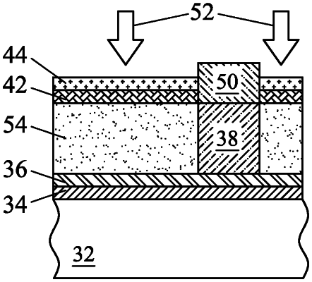
forming over a substrate a layer of photo-sensitive material, the photo-sensitive material having a first dielectric value;
forming a mask over a first region of the photo-sensitive material while leaving a second region of the photo-sensitive material exposed; and
changing the dielectric value of the second region of the photo-sensitive material to a second, lower dielectric value by exposing the second region of the photo-sensitive material to a pre-selected wavelength of light energy, while leaving the dielectric value of the first region of the photo-sensitive material unchanged.
|
|
9. A method comprising:
forming a photo-sensitive material over a substrate;
forming a patterned cap layer over the photo-sensitive material;
using the patterned cap layer, selectively exposing a first portion of the photo-sensitive material to a pre-selected wavelength of light energy to change at least one material property of the first portion of the photo-sensitive material, while leaving the at least one material property of a second portion of the photo-sensitive material unchanged by the exposure process; and
preventing a second portion of the photo-sensitive material from being exposed to the pre-selected wavelength of light energy.
|
|
17. A method of forming a device, the method comprising:
forming over a substrate a layer of photo-sensitive material 38, 78;
forming over a first region of the photo-sensitive material a cap layer 12, 42 the cap layer being transparent to a pre-selected wavelength of light energy;
forming over a second region of the photo-sensitive material a plug 50, 86, the plug being opaque to the pre-selected wavelength of light energy; and
converting the first region of the photo-sensitive material from a dielectric to a conductor by exposing the first region to the pre-selected wavelength of light energy, while leaving the second region of the photo-sensitive material unconverted as a dielectric.
|