| CPC H01L 21/6831 (2013.01) [C23C 14/50 (2013.01); C23C 14/541 (2013.01); C23C 16/458 (2013.01); C23C 16/4581 (2013.01); C23C 16/4586 (2013.01); C23C 16/46 (2013.01); C23C 16/509 (2013.01); H01L 21/3065 (2013.01); H01L 21/31 (2013.01); H01L 21/67103 (2013.01); G03F 7/707 (2013.01)] | 20 Claims |

|
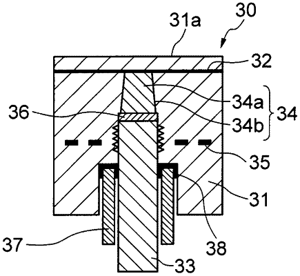
1. A wafer holding unit comprising:
a substantially disk-shaped ceramic substrate having a wafer mounting surface on an upper surface of the substrate;
an electrode embedded within the substrate;
a connecting terminal embedded to have an end surface on one side being in contact with the electrode;
a hole that opens at a lower surface of the substrate to have a bottom surface that is an end surface of the connecting terminal on another side;
a metal member disposed within the hole; and
a metal terminal disposed within the hole,
wherein the hole includes a first inner diameter portion that is positioned on a side of the connecting terminal and a second inner diameter portion that has an inner diameter larger than an inner diameter of the first inner diameter portion, the second inner diameter portion opening at the lower surface,
wherein, at the second inner diameter portion, a tubular sealing member is disposed, the tubular sealing member surrounding the metal terminal,
wherein the wafer holding unit includes a filler in a space formed by a step portion and a forward end of the tubular sealing member, the step portion being positioned between the first inner diameter portion and the second inner diameter portion,
wherein the metal member is disposed between the connecting terminal and the metal terminal to be in contact with both the connecting terminal and the metal terminal, and
wherein the filler is in sealing contact with the forward end of the tubular sealing member and an outermost peripheral surface of the tubular sealing member, and is not in contact with the metal terminal.
|