| CPC H01L 21/465 (2013.01) [H01L 21/6708 (2013.01); H01L 29/66969 (2013.01); H01L 29/7802 (2013.01); H01L 29/872 (2013.01)] | 11 Claims |
|
1. A method of manufacturing a semiconductor device, the method comprising: manufacturing the semiconductor device by:
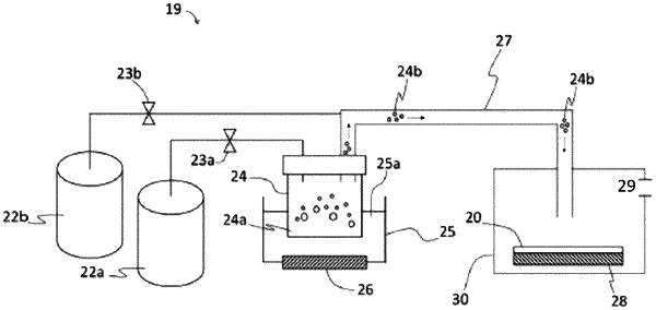
supplying a carrier gas and/or a dilution gas to a mist generator containing an etching liquid;
generating atomized droplets from the etching liquid using an ultrasonic transducer;
supplying the atomized droplets inside an etching chamber onto an object comprising a heated crystalline oxide semiconductor layer and/or a substrate inside the etching chamber; and
etching the object comprising the crystalline oxide semiconductor layer and/or the substrate with the atomized droplets at a temperature higher than 200° C.
|